Contaminating particles on Printed Circuit Boards can have dramatic impact. Such Foreign Object Debris (FOD) can cause shorts, weak solder joints, and voiding.
Fibers and other unwanted particles from bare board manufacturing and dust from transport packaging are frequently found on PCBs.
Laser marking is another source of contamination. In-built vacuum or brush cleaning features often prove to be ineffective.
Many customers are unaware of how dirty boards arrive at the SMT line and are unaware of the associated risks
TEKNEK ‘Board Pack Test’ a Scientific experiment
From experience we know that any PCB arriving from any supplier will contain unwanted debris, many particles even visible to the naked eye. Imagine the potential impact on your assembly!
We can now present the evidence of such contamination, scientifically during an experiment, on site at your facility, on your PCBs.
Partnertec now offers this ‘Board Pack Test’ free of charge to customers in the Benelux, because we believe this is the way to proof that you might need a solution for a problem that you are not aware of yet.
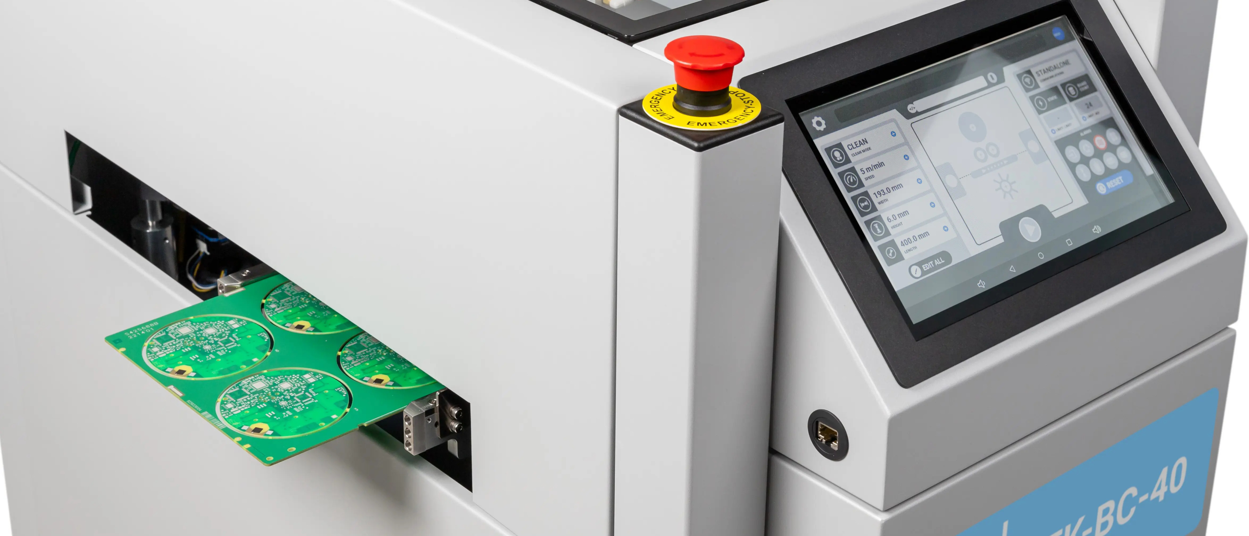
During the test, a manual version of the proven TEKNEK Panel cleaning method will be used. It is ESD safe, causes no strain on your delicate PCBs and uses no cleaning agents, making it completely harmless to your precious boards
The test will take maximum 30 minutes of your time, and all tested PCB’s can be reused in your production, without any risk.
| Book your Board Pack Test Now |