How Multi-level stencils can contribute to better quality
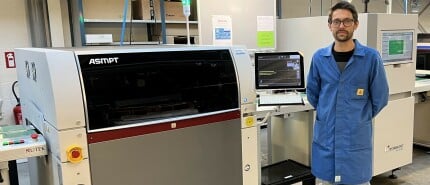
Stencil design and stencil quality have great impact on a stencil printing process and on the quality of assembled PCB’s. Stable and cost-effective printing processes can only be achieved with stencils that are precisely manufactured following correct Design for Manufacturing rules. Partnertec offers a broad portfolio of emulsion screens, laser cut stencils and tensioning frame solutions to match all requirements, ranging from standard SMT applications to the production of the most complex modules and devices.
Benefits of Partnertec standard thickness stencils:
• Based on ASMPT DEK Stencil design knowledge and manufacturing technology
• Latest generation High End Laser Cutting equipment used
• Design for Manufacturing health checks applied
• In depth knowledge of stencil printing in our team
• Available in a wide range of thicknesses and material types
• Excellent print performance
• Minimized Solder Paste waste due to optimized surface structure
• Maximum positioning accuracy
• Compatible with standard mesh-mounted and DEK VectorGuard™ tension frames
Why standard thickness is not always good enough?
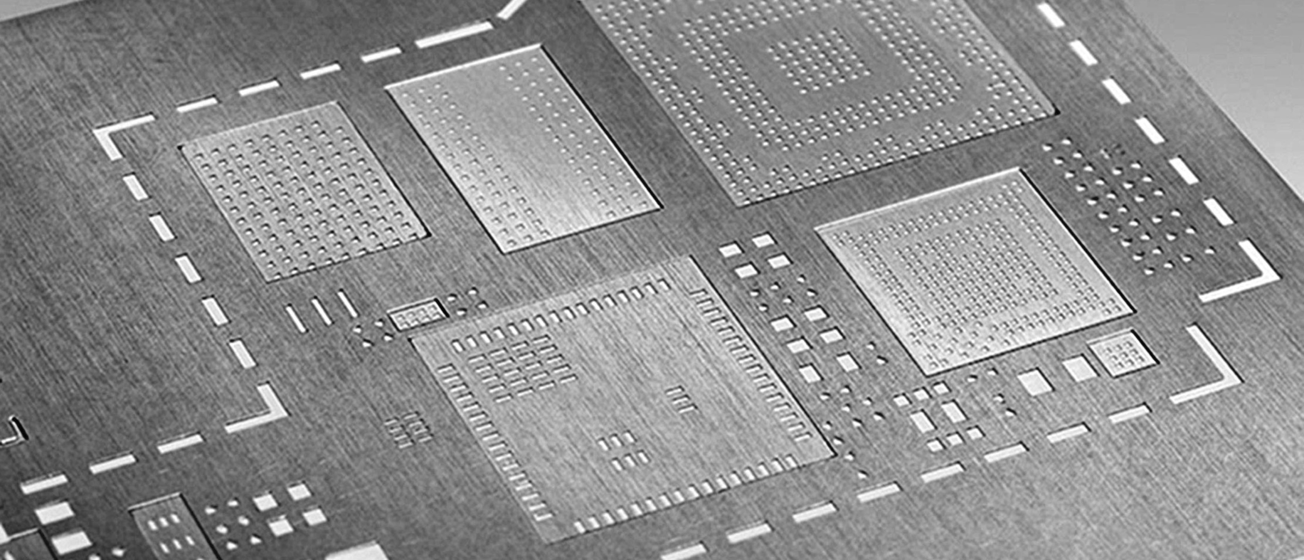
The use of standard thickness stencils however could cause problems on certain components, when the surface area of the aperture in the stencil is too large in relation to the adjacent surface area of the pad on the PCB. If this so called Aperture Area Ratio (AAR) gets too small, solder paste release becomes critical and solder paste might stick to the aperture walls and not release completely from the stencil. This can result in insufficient paste on the pad, causing solder joint defects later on. Reduction of the stencil thickness would resolve the problem but also result in less paste on larger pads, often not accepted for taller components.
To extend the usability of a standard thickness stencils, Fine grain stainless steel and DEK ultra nano coating can stretch the process window and contribute to better paste release. DEK ultra nano coating is not only applied to the stencil surface, but also on the inside of the aperture walls to ensures a better release of solder paste from the stencil. Sometimes a change in the aperture shape can also solve specific issues and our team will always first try to find such solutions first.
But due to the decreasing size of components and increasing high variety of component types a on single board, the optimized and required paste volume for each solder joint cannot always be achieved with a standard thickness stencil.
The solution: Multi-level stencils
To eliminate compromises, Partnertec also offers Stepped Stencils, better called “Multi-level stencils”. Multi-level stencils are produced with the latest high precision technologies such as micro-milling and laser welding to create local step-up or step-down thicknesses in a stencil. Step-up and step-down can also be combined in one stencil. A Multi-level stencil will allow you to optimize the desired amount of paste at all critical areas on your board. Our Multi-level stencils offer extremely tight tolerances for small and large multi-level areas, to allow consistent optimized printing results.
Additional Benefits of Partnertec Multi-level stencils:
• Flexible local adaption to any component mix
• Flexible design of pressure-sensitive areas
• Improved quality by optimized solder joint volume
• Higher first pass yield
• Reduced rework and touch up
• Eliminate need of solder preforms or paste add-on techniques such as jetting and dispensing
• Compatible with standard mesh-mounted and DEK VectorGuard™ frames
For more information and recommendations please contact:
Daan van Hoogstraten - Customer Process Support Manager (dhoogstraten@partnertec.nl)
Sascha Schurian - Senior Stencil Designer (stencils@partnertec.nl)