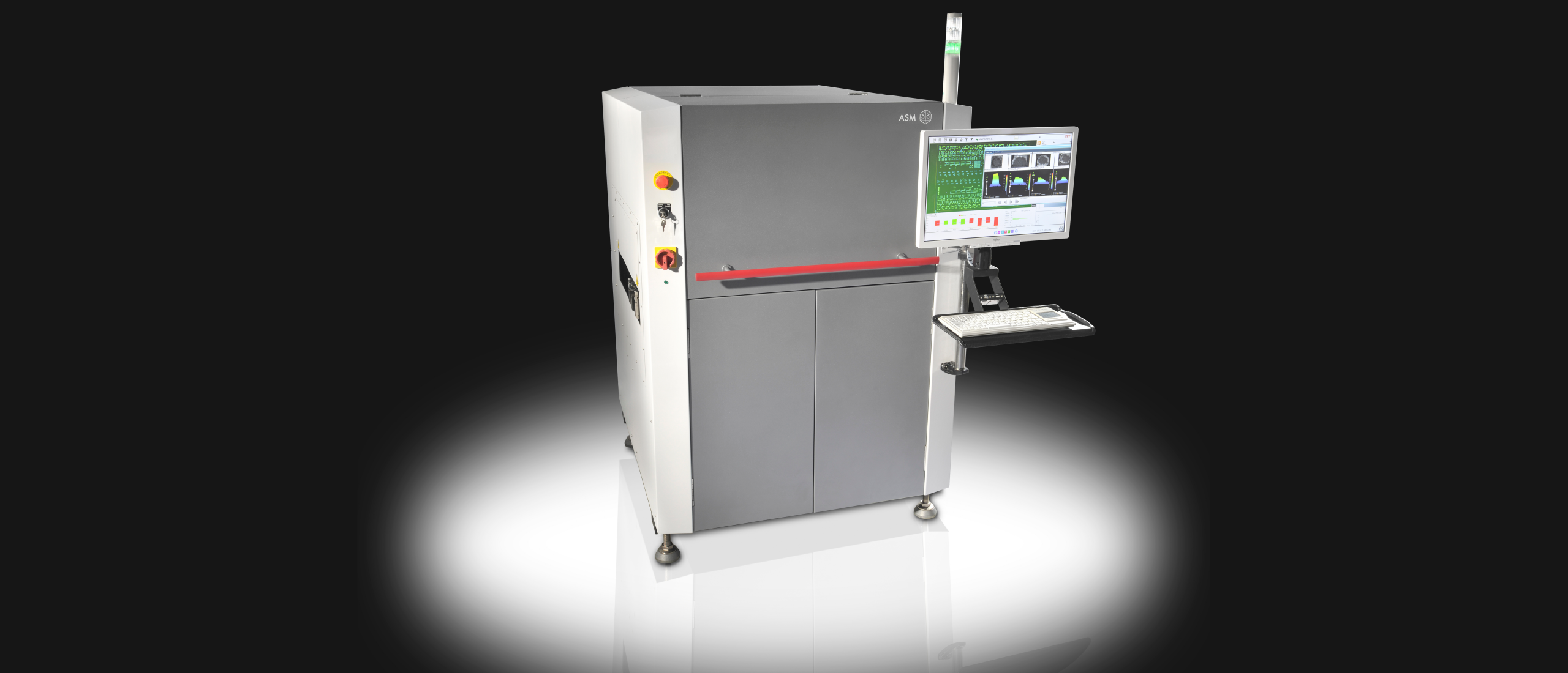
ASMPT has released the HD version of the “Process Lens” - Solder Paste Inspection System
The HD version offers up to 70% faster inspection than traditional inspection systems at much higher accuracy. The new Digital Projection Chip is equipped with 20 million digital controlled micro-mirrors, used to create a very accurate and adjustable Moiré pattern.
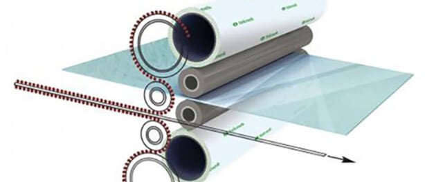
It can measure Solder Paste deposits down to 70 μm x 125 μm size and up to 1000 μm height! 2D analyses, prior to 3D measurement, will eliminate influence from PCB related patterns such as solder resist, tracks or silk screen. Measurement is only made on points of interest such as solder paste, glue dots or unwanted contamination. The machine detects and compensates for board warping, on-the-fly, to assure that the solder paste volume is correctly measured.
In combination with ASMPT ‘’WORKS Process Expert’’ software (see page 2), the system is automatically capable to optimize your stencil printing process completely close-loop. This is done by adjusting all influencing Stencil Printer settings such as print speed, print pressure, separation speed and X-Y offsets. It will also optimize the frequency of under stencil cleaning wipes.
![]()