
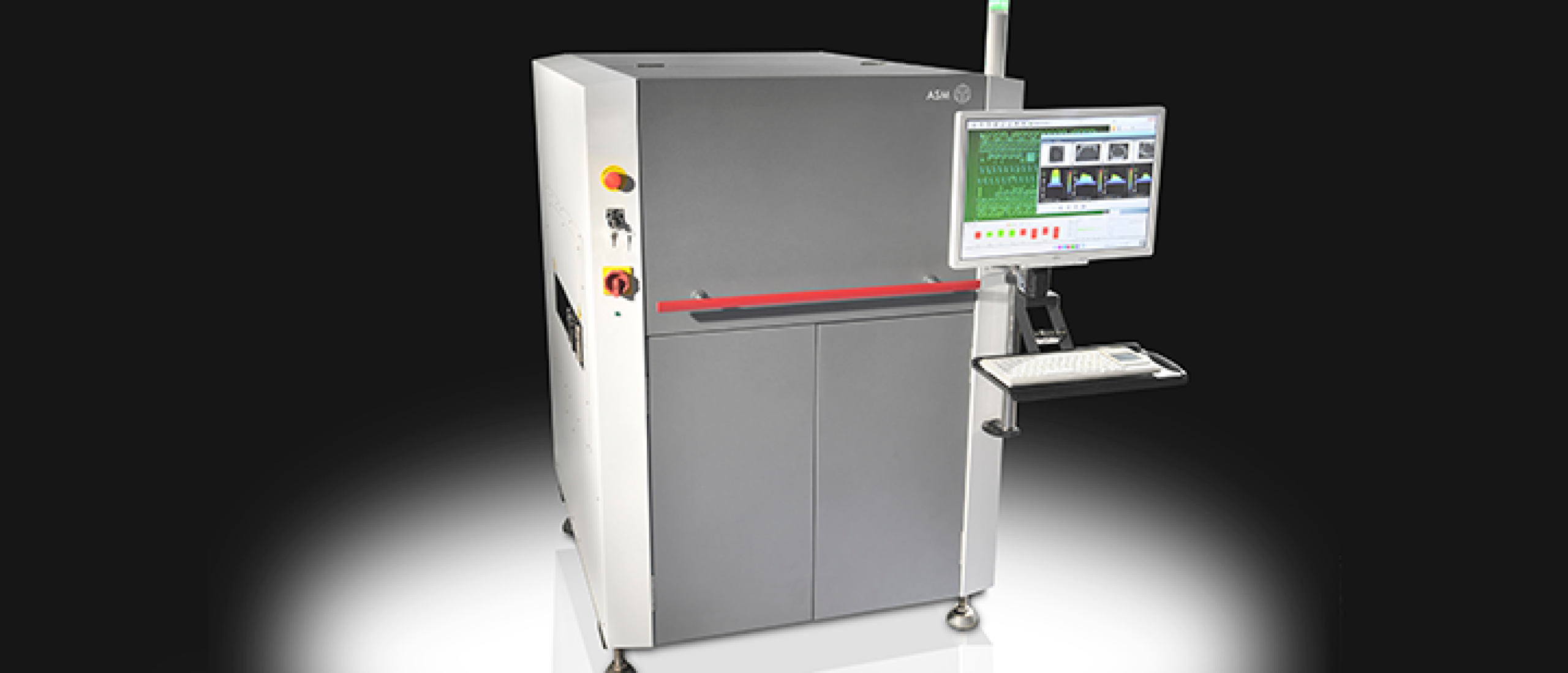
Recently ASMPT has released a next generation SPI that beats all existing technologies. The well-known and established ASMPT Process Lens is now also available in an even faster and more accurate HD version.
It is well known that issues in the stencil printing process contribute up to 60% of the detected End of Line defects. Integrating a Solder Paste Inspection machine (SPI) in the SMD line can avoid expensive rework and improve the Quality.
ASMPT’s SPI systems combine 2D and 3D technologies, to make sure only paste, glue and/or contamination is measured and noise generated by copper tracks, silk screen , solder resist or holes in the PCB is completely filtered out. This results in very accurate measurement data and a drastic reduction of the number of false calls.
ASMPT’s SPI machines are the only systems in the market offering true closed-loop process Control on ASMPT DEK stencil Printers.
Where the existing Process Lens model already uses a very impressive Moiré phase shifting digital light projector with 8 million digitally-controlled micromirrors and camera system, the new HD version goes beyond any imagination.
The new model offers a 50mmx50mm field of view, 25 Mega Pixel camera in combination with a digital projector that uses, mind blowing, 20 million micromirrors to create the desired flexible Moiré projection. This new SPI can achieve up to 70% shorter inspection times and is well able to cope with the output of the fastest stencil printers in the market.
Running in high-speed mode, the system can inspect 90 cm2/s, competing with the fastest laser inspection systems in the market but also offering the great benefits of digital Moiré projection like used in advanced AOI systems.
Running in high resolution mode, this new model offers a 10x10-micron pixel size and allows inspection of the smallest solder deposits, down to 70micron x 125- micron. But the system is also able to measure paste deposits up to 1000 micron height!
Both Process Lens and Process Lens HD can be combined with the advanced self-learning and fully automated Process Expert software, to create a perfect closed-loop process control on ASMPT DEK stencil printers.
The unique approach of ASMPT SPI systems consists of three integrated steps:
STEP 1: DFM analyzes stencil gerber data and recommends the best printer setup and initial printing parameters.
STEP 2: Automated process optimization with a Design of Experiment on the first initial production run and optimize printing parameters.
STEP 3: Proactive control during running production with closed-loop control and continuous improvement on the stencil printer process.
Closed-loop process control and autonomous improvements of the solder paste printing process are only possible when expert knowledge is available to understand how parameter changes affect the printing results. Process Expert’s in-built exhaustive process knowledge database is based on 50+ years of stencil printing experience achieved from ASMPT DEK stencil printing.
The latest version of the software can also import measurement data from third party AOI systems, through the new IPC -CFX data format. This allows faster defect root cause finding analyses on end of line quality issues over the complete SMT line and offers user guidance to improve the entire SMD assembly process.
Please let us know if you would like to learn more about how ASMPT Process Lens and Process Lens HD can help you to improve your SMD assembly process.
Follow us to receive the latest news!
Follow us to receive the latest news!
<:optin-form-placeholder>
Introduction of the most advanced Solder Paste Inspection system ASMPT process lens HD

Place comment